


 Abstract
 HTML
HTML Reference
 Related
 PDF
PDF


-
The
229 Th nucleus has a unique low-lying isomeric state with the energyEis , which is equal, according to the latest data, to8.19±0.12 eV [1]. The history ofEis measurements made in the last five decades, from the first values ofEis≤100 eV [2],Eis=1±4 eV [3], and3.5±1.0 eV [4] via the values7.6±0.5 eV [5] and7.8±0.5 eV [6] to the currently accepted valuesEis=8.30±0.92 eV [7],Eis=8.28±0.17 eV [8],Eis=8.10±0.17 eV [9], and8.19±0.12 eV [1], has already been described repeatedly and in great detail in various works (see, for example, [7, 9, 10] and references therein).Interest in the isomeric level in
229 Th lies primarily with the possibility of creating an ultraprecise nuclear clock [11–17] and a γ-ray laser of optical range [18] based on the inversion population of the levels in the low-lying doublet in229 Th [19, 20]. The nuclear ultra-stable optical clock is of interest to a number of fields of physics. With its use, we will be able to conduct research on the effects of the Einstein Equivalence Principle and local Lorentz Invariance violations [21], to study the relative effect of the variation of the fine structure constante2 and the strong interaction parametermq/ΛQCD [22–25], for dark matter searches [26]. Alongside these important challenges, the low-lying isomer of229 Th allows us to explore the exotic process of decay and excitation of the nucleus via an electron bridge [27–35], accelerate the α decay of the229 Th nucleus [36], control the isomeric level of γ decay via the boundary conditions [37], detect229 Th ground state decay into the isomeric level in the(μ−1S1/2229 Th)∗ muonic atom [38], investigate the229m Th decay through the metal conduction electrons [39], observe the Zeno effect [20], etc.The most efficient method of excitation by resonant laser photons in the process of direct photoexcitation of
229m Th [31] or excitation via the electron bridge [28–41] is currently impossible. These methods require precise tuning of laser radiation to an unknown wavelength of the nuclear transition or stimulation of an atomic M1 transition close in energy to the nuclear transition in the process of nuclear excitation by electron transition (NEET see in [42–44]), which is the "second stage" of the excitation of229m Th via the electron bridge. However, it should be noted that the excitation of the229m Th isomer in the process of direct photoexcitation of the 29 keV level, first proposed and theoretically substantiated in Ref. [45], has already been successfully implemented experimentally [46].Registration of photons from the decay of
229m Th could immediately determine the energy of nuclear transition with high accuracy in a low-lying doublet of levels of the229 Th nucleus and open the path to resonant pumping of the isomer. The first successful observation of the gamma decay of the229m Th isomer accompanying the beta decay of229 Ac, implanted into a large-bandgap dielectric, was reported in Ref. [47]. Another type of experiment to observe the gamma decay of229m Th (produced by the alpha decay of233 U) in an ion trap is described in Ref. [48].In this study, we propose an algorithm for the solution of one main problem in this field of modern science, namely, the excitation of the
229m Th isomer in the solid state (dielectric matrix) by electron current and creating a source of γ quanta of the VUV range, which accompanies isomeric decay of229m Th. -
The low-energy isomeric transition in
229m Th has a high probability of internal conversion [27, 49–51]. It was the measurements of the conversion electrons energy in works [8, 52] that gave one of the modern values forEis . However, the internal conversion makes registration of photons almost impossible. The solution to the problem was described in Refs. [45, 53, 54]. These studies have shown the decay of229m Th in dielectrics with a large bandgap, Δ, to occur precisely with the photon emission and the internal conversion atEis<Δ to be forbidden energetically. In a wide-gap dielectric, thorium participates in chemical bonds by donating electrons. The described efficient ionization increases the binding energies of the remaining electrons. It proves to be sufficient to stop the decay of229m Th via the internal conversion channel.The last missing link, namely, an efficient way of non-resonant excitation of the
229m Th isomer, was recently proposed in Ref. [10]. The cross sections for inelastic scattering of slow electrons with energies of about 10 eV turned out to have reached values (2–6)×10−26 cm2 depending on the value of the nuclear matrix element. These are rather large cross sections by nuclear standards. It is essential that they make it possible to excite the229 Th nucleus even if the exact value of the nuclear transition energy is not known. For comparison, the typical effective cross section of resonant photoexcitation of the isomer by laser radiation with a linewidth ofΔlas≃10−10 eV, calculated from the formulaσeff=(λ2is/2π)[Γγ(M1,gr→is)/Δlas ], whereλis=2π/Eis andΓγ denotes the radiative transition width (see below), is (2–8)×10−20 cm2 . However, as we noted above, for resonant photoexcitation, it is necessary to know the wavelengthλis with high accuracy.Now let us see how these problems can be circumvented using a relatively simple scheme. We consider the layout of the device in Fig. 1. Here,
229 Th is implanted into a thin dielectric layer with a thickness h on the order of 10–20 nm with a large bandgap. Currently, there are several dielectrics of this type: SiO2 [55], CaF2 , LiCaAlF6 , LiSrAlF6 , Na2 ThF6 , LiYF4 [12], and MgF2 [56]. Voltage is applied to the dielectric through a metal contact on one side and a doped semiconductor (Si for example) or a metal contact on the other side. Note that, if silicon is used as a semiconductor, it is quite easy to grow a thin dielectric SiO2 film directly on an Si substrate. Depending on the doping material, it is possible to prepare an n-type or p-type semiconductor with the appropriate current flow direction in the device. To be more specific, an n-type semiconductor is shown in Fig. 1.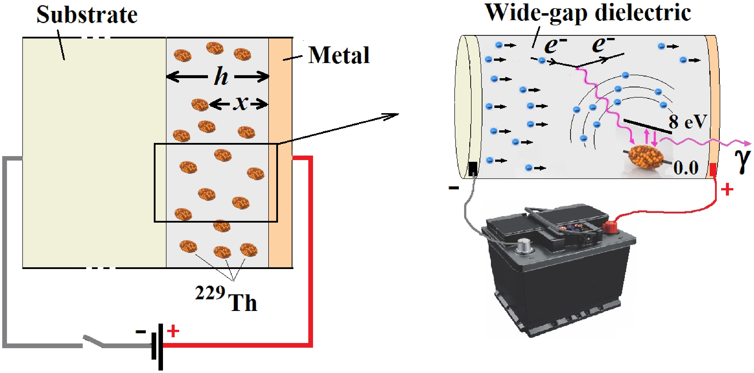
Figure 1. (color online) Nuclear light source based on
229m Th. The left part is a diagram of the device, and the right part is the excitation of229 Th by the electrons and the emission of γ quantum during the transition of the nucleus to the ground state. "Metal" designates a sputtered thin metal contact (Pd and Au were taken for numerical estimates in this work). SiO2 and MgF2 were considered as large band gap dielectrics (they can be replaced by another dielectric with a large band gap). Doped Si and Au were taken as the substrate.As we already noted, the dielectric film should be thin enough to allow the passing of electric current. Its optimal thickness is no more than a few electron mean free paths. Thin films of 10-30 nm are convenient for the following reason. The
229m Th isomer excitation cross section for inelastic electron scattering reaches a maximum at energies of 9–10 eV [10]. Therefore, it is reasonable to work with an electrical potential difference between the contacts at a level of several tens of volts (before an electrical breakdown occurs, which leads to material degradation, the dielectric strength of SiO2 is approximately 4 GV m−1 [57]; with the film thickness of 10 nm, the breakdown voltage is 40 V). Under such conditions, the transport of electrons through a thin dielectric film occurs due to the tunneling process (practically, this is the process of electric field electron emission). Thicker films can also be used, but to ensure tunneling, a higher electric potential difference between the contacts should be applied. As a result, the region in which the electron energy is much higher than the optimal one will be significantly increased in size (see below).Therefore, the applied voltage is selected so that the electrons scattered by the
229 Th nuclei have a kinetic energyEkin that is sufficient to excite the nucleus. In the scheme in Fig. 1,Ekin∼(qe/n)V(x/h) , where V is the applied voltage in volts, dimension ofEkin is electronvolts, x is the depth counted from the electron entry point into the film,qe is the elementary charge in units of electron charge, and n is the refractive index of the dielectric film. Assuming that, at the initial time, the229 Th nuclei are distributed over the dielectric layer thickness with a certain densityngr(x) , and that the main voltage drops precisely on the dielectric film, we find the condition necessary for the excitation of nuclei at depth x:V≥(n/qe)(h/x)Eis . In other words, in order for the excitation reaction of the nucleus to proceed, for example, in half of the dielectric layer, it is necessary to apply the voltage in voltsV=2nEis/qe , whereqe=1 . -
Let us estimate the γ activity of isomeric nuclei excited according to the given scheme. Let the density of the
229 Th nuclei in the target sample at depth x bengr(x,t) , and the density of the resulting229m Th isomers benis(x,t) . The equations describing the system are as follows:dnis(x,t)/dt=σφngr(x,t)−(λtot(x)+˜σφ)nis(x,t),dngr(x,t)/dt=−σφngr(x,t)+(λtot(x)+˜σφ)nis(x,t),

(1) where σ is the isomer excitation cross section for inelastic electron scattering in the process of
229 Th(e,e′) 229m Th,˜σ is the cross section of the reverse process (calculated from the principle of detailed balance and coincides in order of magnitude with σ [10]),φ=j/S is the electron flux density through a target with area S when passing the current j, andλtot(x) is the total decay constant or isomeric state width (with using the unit systemℏ=c=1 ) in the sample at depth x. The expressions in Eq. (1) are solved with initial conditionsnis(x,0)=0 andngr(x,0)=ngr(x) . It should also be noted that the electron flux density of a given energy φ is practically independent of x due to the small thickness of the dielectric layer.Let us simplify Eq. (1). 1) We neglect the decrease in the density of the
229 Th nuclei in the ground state with time, that is, letngr(x,t)=ngr(x) . 2) We discard the term−˜σφnis(x,t) , which describes the inverse process229m Th(e,e′) 229 Th of nuclei deexcitation during inelastic electron scattering. These simplifications are to be made as the conditionσφτ≪1 is met for the considered current density of the order of 1 A cm−2 (in this case,1/(σφ)≳106 s) and the expected lifetime of the isomeric stateτ(x)=1/λtot(x)≃102 –103 s (see below). On the one hand, this condition implies that the main decay channel for229m Th is the spontaneous decay of the isomeric level, and not the transition to the ground state upon inelastic electron scattering. On the other hand, the density of the excited229m Th nuclei at depth x increases according to the characteristic lawnis(x,t)=ngr(x)σφλtot(x)(1−e−λtot(x)t),

(2) where
σφ/λtot(x) is the relative equilibrium concentration of isomeric nuclei at depth x at timest≫τ . In order of magnitude,σφ/λtot(x)≃10−4 , and densityngr(x) does not change much with time.Now let us return to the question of the value
τ(x) . For this, we first estimate the characteristic radiative width of the isomeric stateΓγ in vacuumΓγ=10ω3γμ2NBW.u.(M1,is→gr),

where
μN is the nuclear magneton, andM1 is the multipolarity of isomeric transition.In order to calculate
Γγ , it is necessary to know the reduced probability of nuclear transition in Weiskopf unitsBW.u.(M1,is→gr) . In Ref. [58], the valueBW.u.(M1,is→gr)=0.03 was obtained based on experimental data [59–62] for theM1 transitions between the rotation bandsKπ[NnzΛ]=3/2+[631] and5/2+[633] in the229 Th nucleus and the Alaga rules [58, 63]. Here,Kπ[NnzΛ] are the asymptotic quantum numbers for nuclear levels in the Nilsson model [64]). The other value,BW.u.(M1,is→gr)=0.006−0.008 , was obtained in Ref. [65]. It was the result of a computer calculation made in compliance with modern nuclear models. These two values forBW.u.(M1,is→gr) give the time intervalT1/2=ln(2)/Γγ= 20–100 min for the radiative decay of the isomer in thorium ions in vacuum at the nuclear transition energyωγ=Eis=8.2 eV.The probability of decay of the
229m Th isomer in the sample in Fig. 1 is influenced by two factors — the refractive index of the medium [45, 53] and the presence of interfaces between the media (the Purcell effect) [37]. The probability of magnetic dipole (M1 ) γ radiation of229m Th in a medium with a refractive index n increases byn3 times compared to the probability of radiation in vacuum [45,53]. The Purcell factor,fP(x) , that is the ratio of the probability of emission in a medium with boundaries to the probability of emission in an infinite medium, affects the decay of229m Th more intricately. Figure 2 shows the Purcell factors for theM1 γ transition with the energy of 8.2 eV for the system shown in Fig. 1. The calculation was made within the framework of the approach developed and described in detail in Ref. [66] (we provide a graphical representation of the result, since the analytic expressions forfP(x) for four media are highly complex). Pd and Au were taken as examples of the deposited metal contact. Their characteristics, namely,n=1.3 andκ=0.9 for Pd andn=1.3 andκ=1.5 for Au at the energy of 8.2 eV, are given in Ref. [67]. The thickness of the Pd or Au layers is estimated to be equal to 10 nm. It is limited by the requirement of contact transparency for VUV photons. The fraction of the incident power, propagated through the material with thickness d, is given by exp(-d/l0 ), wherel0=λisκ/(4π) andλis≈150 nm. Using the values of κ for Pd and Au from Ref. [67] given earlier, we find that, in a metal layer of thickness 10 nm, the VUV photon flux is attenuated by a factor of approximately 3 for Pd and 2 for Au.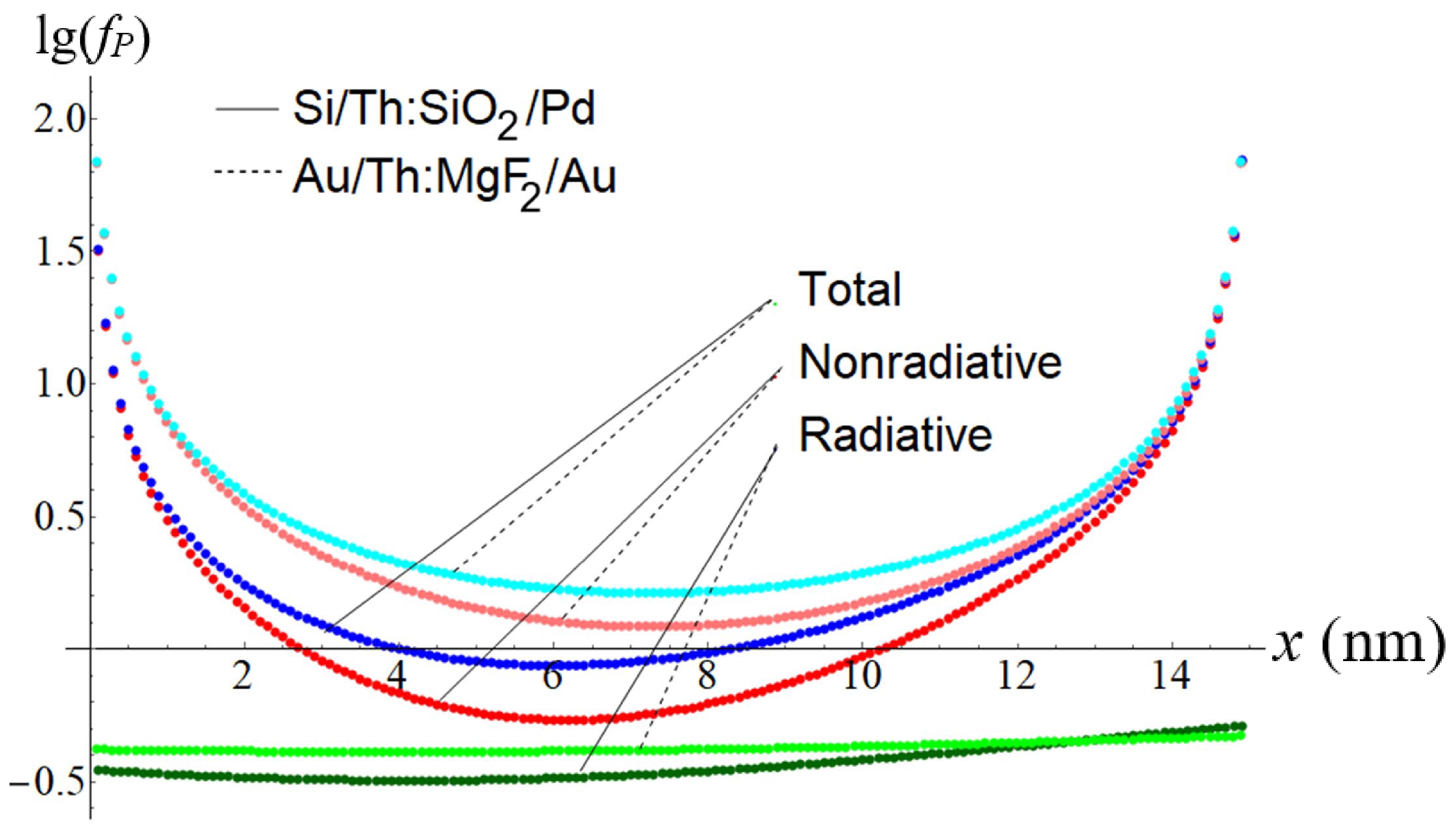
Figure 2. (color online) The radiative,
frP(x) , nonradiative,fnrP(x) , and total,ftotP(x)=frP(x)+fnrP(x) components of the Purcell factors for theM1 (8.2 eV) γ transition in the scheme in Fig. 1 withh=15 nm for thickness of the large band gap dielectric and 10 nm metal layer thickness. The thickness of the substrate in calculations is assumed to be infinite. Solid lines — the Si/229 Th:SiO2 /Pd sample and dashed lines — the Au/229 Th:MgF2 /Au sample.At the SiO
2 /Metal interface, there are surface states whose levels are located inside the SiO2 band gap. The presence of these levels can lead to an increase in the probability of the isomeric decay of229m Th through the internal conversion or electron bridge for the thorium atoms located within 2–3 monolayers from the interface. Additional losses in the photo output can be avoided by lowering the concentration of thorium atoms in the near-surface layer so that the doping profile reaches a maximum at a depth of approximately 1 nm (of the order of 3 coordination radii). In the case of a uniform distribution of229 Th, this problem will affect 10–15% of the nuclei, reducing the optical output by the same amount.Figure 2 shows the probability of radiative decay determined by
frP(x) to decrease due to the interfaces Pd/SiO2 (x=0 ) — SiO2 /Si (x=h ) and Au/MgF2 (x=0 ) — MgF2 /Au (x=h ). However, the total decay probability increases significantly due to the factorfnrP(x) . It characterizes the nonradiative decay of229m Th, which arises from the imaginary part of the dielectric constants of Si, Pd, and Au [66]. As for the silicon oxide, the imaginary part of the dielectric constants of SiO2 lies in the range of 0.02–0.03 at the energy of 8.2 eV [68, 69]. Thus, κ is very small for SiO2 , and it can be neglected in calculations. For MgF2 κ≈3×10⁻⁷ at 8.2 eV [68].With respect to these factors, it is possible to derive the formula for the total γ activity caused by an electric current in the entire sample
Qγ(t)=σφS∫h0dxngr(x)frP(x)ftotP(x)(1−e−λtot(x)t),

where
λtot(x)=n3ftotP(x)Γγ .Figure 3 shows the graphs of induced activity.
Qγ for the sample from Fig. 1 is seen to behave much more differently than the γ activity of an equivalent target of229 Th+,++... ions in vacuum or in an infinite medium of SiO2 or MgF2 . Both the emissivity and the observed effective half-life of the entire set of isomeric nuclei change significantly.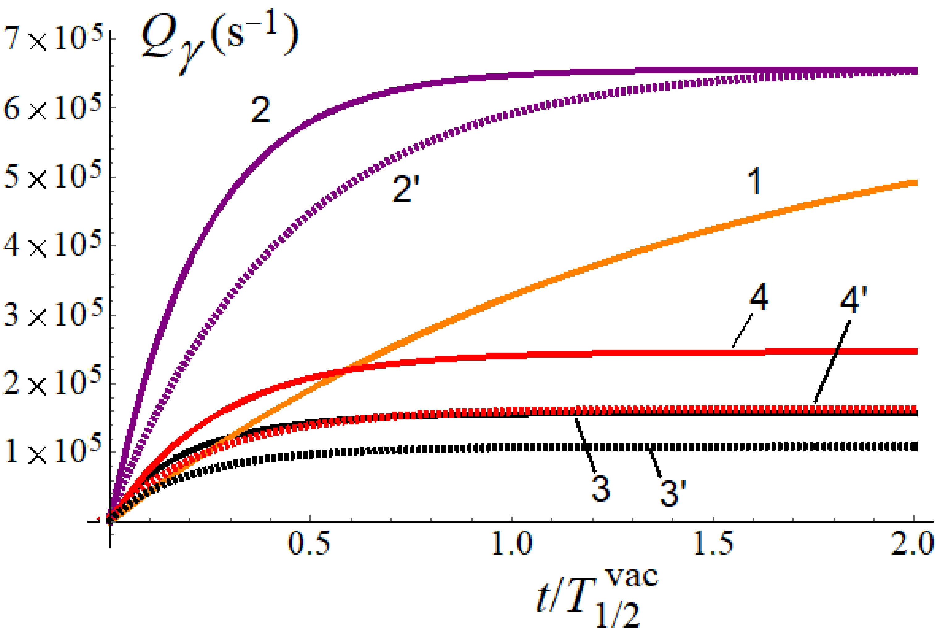
Figure 3. (color online) The γ-activity of the sample per 1 A of electric current and per 1 ng of
229 Th as a function of the irradiation time. 1 — the229 Th+,++... ion target in vacuum, 2 (2') — the same target in the infinite medium of SiO2 (MgF2 ), 3 (3') — the229 Th target in the Si/Th:SiO2 /Pd (Au/Th:MgF2 /Au) sample in Fig. 1 with a uniform distribution of nuclei in depthngr(x)=Const=Ngr/(hS) (Ngr is the total number of229 Th nuclei implanted in a dielectric layer), 4 (4') — all the229 Th nuclei located in a thin layer inside SiO2 (MgF2 ) at a depth ofx≈6 nm, where the functionsfnrP(x) have a minimum value (this is a type of upper limit for the γ-activity for the sample in Fig. 1).As can be seen from Fig. 3, gamma activity in the sample upon reaching equilibrium at times
t≈T1/2/2 is approximately105 photons/s per 1 A of electric current and 1 ng of229 Th.229 Th is an α emitter withT1/2=7880 yr. Alpha particles, decelerated in SiO2 (MgF2 ), produce a background radiation. Alpha activity of 1 ng of229 Th is 7 Bk. The mean free path of α particles with the energy 4–5 MeV in SiO2 (MgF2 ) is approximately 20 μm. With a dielectric layer thickness of 15 nm, only10−3 α particles lose energy in the dielectric and contribute to the background (alpha particles in the Si (Au) substrate and metal contacts do not produce an optical background). Assuming that the ionization potential is 10 eV, and that all energy of the alpha particles is converted into photons, we get a background of approximately103 photons per second, per 1 ng of229 Th purified from daughter nuclides. This means that we can secure two orders of magnitude for current, until the signal falls to the background level.Let us compare this estimate with the background from
233 U. To have the same number of the 8.2 eV γ quanta as from 1 ng of229 Th, the α activity of233 U should be at the level of105× 50 (taking into account the 2% isomer population). This requires approximately 140 mg233 U. In this case, the host crystal will have a volume of at least10−1 cm3 . Alpha particles will be completely decelerated in such a crystal and leave all their energy in it. Thus, other things being equal, the background for233 U exceeds the estimate obtained for 1 ng229 Th by 8 orders of magnitude. This underlies the advantage of using the proposed scheme with thorium.Another source of the background radiation could be the electron flux through the carrier substrate. In this case, the radiation in the vacuum ultraviolet range comes from the processes of exciton recombination. In experiments specifically carried out in 2021, it has been found that, in the Si substrate and SiO
2 matrix, the emerging background in the wavelength region around 150 nm is very small and only slightly exceeds the intrinsic noise of the detector [70].The emission line from the isomeric decay of
229m Th is planned to be registered using the same setup that was used to measure the background. The setup device is as follows. A converging short-focus lens made of a material transparent in the VUV range (MgF2 ) is placed in front of the sample. A focused beam of light falls on the slit of a diffraction spectrometer. The spectrometer is made according to the Paschen-Runge optical scheme, in which the entrance slit of the spectrometer and the spherical diffraction grating are located on the Rowland circle, and the radiation from the entrance slit falls almost normal to the diffraction grating. This scheme has the following advantages: 1 - only one reflection is used, which makes it possible to minimize the loss of incoming radiation; 2 - it is possible to change the grating tilt to capture the desired part of the spectrum, which allows us to measure spectra in a wide range.The background spectrum and the
229m Th radiation wavelength are determined from the diffraction pattern using a charged-coupled device (CCD) matrix cooled to a temperature of -20∘ C under vacuum conditions no worse than10−8 Torr. With the CCD matrix, we can accumulate the signal simultaneously (without scanning) over all channels of the selected region of the spectrum, which in turn allows for measuring the emission spectrum with a high decay rate over time. The maximum luminosity of the spectrometer reaches104 (i.e., one photon is registered out of every104 photons arriving at the spectrometer input).The experiment can be carried out in two modes. (1) Registration and measurement of the spectrum occur directly during the passage of electric current through the sample. (2) Registration occurs after the electron current is turned off and after the completion of the relaxation of electron-hole pairs and other transient processes — the background sources. In both modes of operation, to take into account the background correctly, it is necessary to carry out measurements on samples without
229 Th. Such a scheme allows us to separate photons originating during the decay of the229m Th isomer from the contributions of all other possible electronic transitions in the Th shell. The background accumulation time is required to correspond to the useful signal accumulation time (see Fig. 3), i.e., approximately103 s. The described sequential consideration of the signal from samples with229 Th and232 Th will single out the desired emission line of the229m Th isomer.Consider the size of the sample in Fig. 1 in terms of the allowable concentration of the thorium atoms. Let us take SiO
2 as an example, since we have all necessary data for it. According to the results of Ref. [71], where thorium ions are implanted into SiO2 , thorium is oxidized to the ThO2 form. The ThO2 band gap is approximately 6.5 eV. Therefore, the appearance of the ThO2 impurity in SiO2 leads to a decrease in the band gap of the sample as a whole. It was theoretically and experimentally established in Ref. [71] that, up to a thorium concentration of 20%, the band gap in such SiO2 +ThO2 dielectrics exceeds 8.5 eV. Thus, in a dielectric matrix of the size 1 cm2× 15 nm, approximately 10 ng of229 Th can be placed (note that, in the theoretical work of a group from the Vienna University of Technology, it has been found that the band gap of thorium-doped MgF2 decreases with the concentration of thorium [56].)As a result, we obtain the following estimate: at a moderate current of 1 A, detector quantum efficiency
≳10−1 , and photon collection angle≈2π , the γ radiation detector registers approximately104 –105 counts/s from such a matrix, which is sufficient for the effect to be reliably detected above the background level. -
The described scenario is plausible only if there are no additional electron levels in the band gap of the dielectric matrix containing
229 Th. These can be impurity levels or lattice defects, formed in processes such as thorium implantation or α decay of the229 Th nuclei. Such additional electron states of different nature formed inside the band gap in the process of target fabrication can cause a rapid decay of the229m Th isomer through an internal conversion channel or via the electron bridge. This can negatively affect the yield of the nuclear light source. The issue of such additional levels was studied in Refs. [12, 47, 54, 71–76]. In particular, as shown theoretically in Ref, [76], a set of electronic defect states in the229 Th:CaF2 crystal band gap (229 Th-doped CaF2 ) leads to excitations via the electronic bridge mechanism, which proceed at a rate 2 orders of magnitude larger than the direct photoexcitation of the isomeric state.It is important to note that, depending on the thorium concentration, dielectrics seem to behave differently. The band gaps of thorium-doped CaF
2 and MgF2 decrease with the concentration of thorium [56, 71]. Nevertheless, the experimental results of Refs. [12, 47, 71, 74, 75] are promising. These studies developed dielectric matrices LiCaAlF6 , CaF2 , SiO2 , and MgF2 with thorium without additional states in the band gap. This means that the presence of a thorium dopant in the proper concentration in these crystals does not lead to the appearance of additional electronic levels inside the bandgap, and that the bandgap width, Δ, remains quite large, exceeding the energy of the isomeric nuclear transitionEis . This important issue should always be focused on during sample preparation.Another problem with thin films on substrates is the mismatch between crystal structures and lattice constants of the film and the substrate. For the MgF
2 /Si system, this effect should be taken into account. However, this is a separate technological problem, which we do not consider here. As for the SiO2 /Si system, it is convenient to use the amorphous SiO2 film obtained by the thermal oxidation of silicon. This technology is well established in microelectronics, and it can be used to obtain thin silicon oxide films of high dielectric quality with a large band gap (≃9 eV) [77]. -
The proposed scheme can be considered as a nuclear counterpart of a conventional light source. Nuclei are excited as a result of inelastic scattering of electrons. This is a non-resonant threshold process, which, most importantly, does not require precise tuning to an unknown nuclear transition energy, but at the same time, produces a sufficiently large number of excited nuclei. As a result, there is a real possibility of detecting γ quanta from the nuclear isomeric transition in
229 Th.
Proposal for a nuclear light source
- Received Date: 2022-10-08
- Available Online: 2023-02-15
Abstract: This study considers a principal possibility of creating a nuclear light source of the vacuum ultra violet (VUV) range based on the


 DownLoad: